

Proterial Metals, Ltd. TOP > Products > Metals for Communications, Semiconductors and Packages
> Au coated Ni-P particles
Metals for Communications, Semiconductors and Packages
●Au coated Ni-P particles
【Features】
Packaging technologies for those devices have also been evolving towards higher performance and higher density.
We manufacture these highly conductive fine particles of uniform size by wet reduction method, which was developed jointly by Group Company and Akita Prefectural Resources Technology Development Organization.
It is a potential technology that enables the higher performance and higher density required for next-generation electronic components.
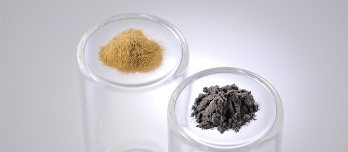
【Product image】
【Applications】
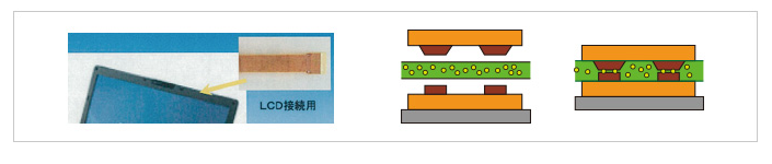
- ・Display / Semiconductor Package Components and Spacer
【Technology】
- ・Metal ball manufacturing process
- ・Plating(Au, Ag, Solder etc.)
【Usage example】
【Technical report】
Demand for erectric devices, including smartphones and tablet PCs, has been growing rapidly. It is expected to continue growing, mainly in emerging countries.
Erectric devices are evolving towards higher resolutions, multifuntional, and lower profiles. Packaging technologies have also been evolving further towards higher performance and higher density.
In this trend, there is a growing demand for precise gap control between substrates and IC chips and anisotropic conductive connections between substrates.
From collaboration with Akita Prefectural Resources Technology Development Organization, Our group company has developed a wet reduction method for manufacturing spherical metal particles.
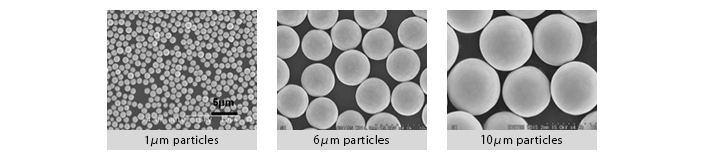
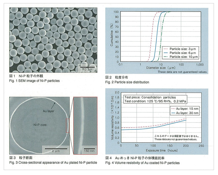
As shown in Figure 1, the particles having smooth surface are completely spherical, uniform in size, and highly dispersive. The limited variation in the particles is also apparent from the result of the measurement of particle size distribution with the laser diffraction method shown in Figure 2.
In addition, conductive fine particles are required to maintain stable conductivity, even in a harsh environment. In response, we have established a uniform Au plating technology to plate large quantities of fine Ni-P particles having large specific surface area, which has been deemed difficult. It can be confirmed from a cross-sectional image of the film formation of Au plating, which is shown in Figure 3, that an Au plating layer of an even thickness is formed on the particle surface. And it was confirmed in an accelerated test (125ºC/95 RH%, 0.2 MPa; RH stands for relative humidity), by which we evaluated the changes of particles, that the volume resistivity increases only around two times compared to the initial resistivity even when the Au film around the particle is extremely thin at 15 nm or 30 nm (Figure 4).
Cuurently, we can offer fine unified particles with high conductivity and high corrosion resistance plating in the range of 1-20μm in diameter.
Please feel free to make an inquiry.
- Products
-
- Metals for Environment and Energy
- Metals for Automobiles
- Metals for Communications, Semiconductors and Packages
-
- Iron-Nickel-Cobalt alloys
- Iron-Nickel alloys
- Low thermal expansion alloys for precision equipment
- Permalloys
- Clad metals for heat spreaders
- Metals for laser diodes
- Clad metals for smartphones
- Bimetals
- Metal parts for package sealing
- Au coated Ni-P particles
- Lead pins
- Metals for functional parts
- Copper alloy strip for semiconductor lead frames
- Dual gauge copper strip
- Plated copper strip and dual gauge copper strip
- Copper strip for heat sinks and heat spreaders
- Copper strip for ceramic substrates
- General industry
- Metals for Domestic Electrical Applications
- Metals for Special Applications
- Material technologies
-
- Material technologies
- Processing technology
- Surface treatment technologies
- Corporate Profile
- Contact Us
PAGE TOP
COPYRIGHT ©Proterial Metals, Ltd.
ALL RIGHTS RESERVED.